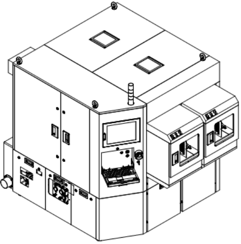
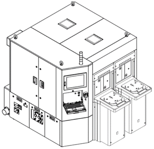
DY-2000RC/DY-3000RC Equipment Features
-
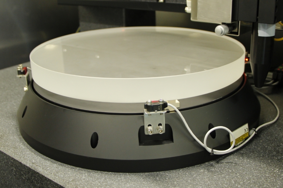
Capable of measuring wafers up to 300mm (12inch) in diameter
Using the SORI measurement data before and after deposition, the software specifies analysis lines in the wafer diameter direction and calculates the film stress distribution according to the radius of curvature and set parameters for each data. It also calculates profile data for each cross-section and outputs a report. High throughput measurement of the entire wafer surface is possible by spiral scanning the wafer at high speed.
-
This device is designed to comply with various safety standards to ensure safe use.
Supported Standards
- ・SEMI S2-0818
Environmental, Health, and Safety Guidelines for Semiconductor Manufacturing Equipment - ・SEMI S8-0218
Safety Guidelines for Ergonomic Engineering of Semiconductor Manufacturing Equipment - ・ISO 12100
Safety of Machinery - Design Principles - ・IEC 602040-1
Safety of Machinery - Electrical equipment of machines -
- ・SEMI S2-0818
-
-
Analysis Software
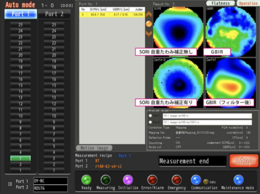
Various measurements such as 2D/3D cross-sectional profiles using measurement data and various analyses such as Semi standard "SORI", "Bow", "Warp", and "GBIR" are performed. Export to CSV file and report output are also available.
-
Self-weight Deflection Compensation
By using the measurement data to compensate for deflection caused by the wafer's own weight, the original wafer deflection data can be calculated. This is especially effective for thin wafers and large diameter wafers.
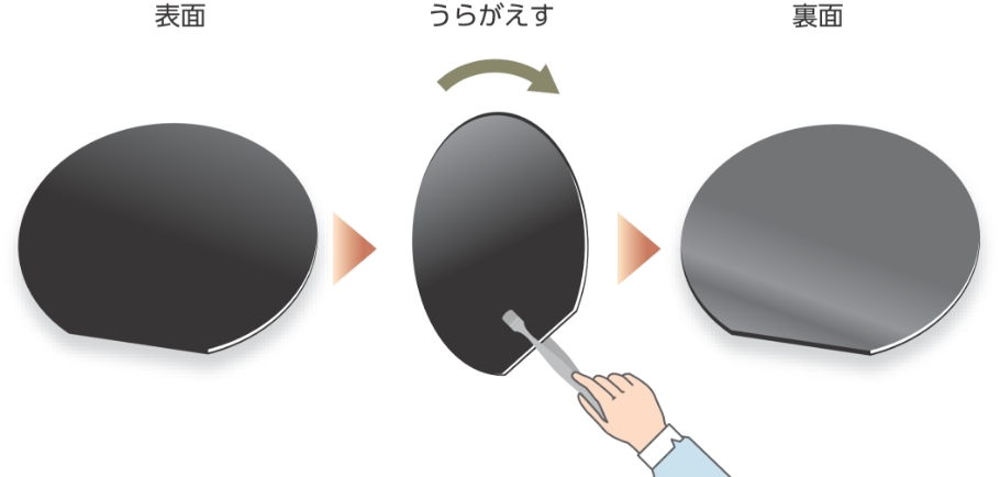
Double-sided Differential Mode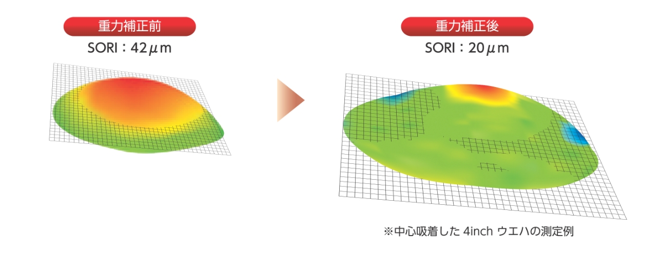 Ideal Model Difference Mode
The surface profiles of the back and front surfaces of a wafer are measured, and the difference between the data is used to create correction data that eliminates the effect of self-weight deflection.
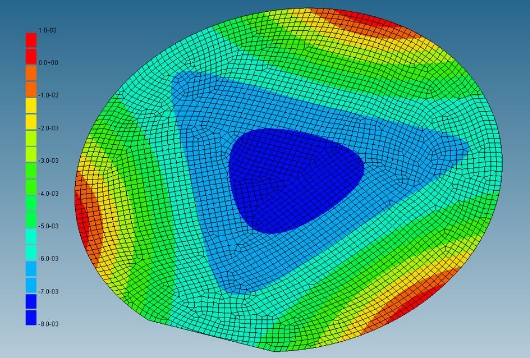
The difference between the ideal model of a wafer including self-weight deflection created by the finite element method and the measurement data is used to create correction data that eliminates the effect of self-weight deflection.
-
Correction function using reference gageCorrection Using Reference Flat Substrate (Mapping Correction)
The surface height data of the reference plane substrate is measured in advance and used as correction data. By subtracting the correction data from the actual workpiece measurement data, the minute oscillation of the scanning stage is compensated and the true value of the workpiece is approached. This is especially effective for measurement of workpieces with small warpage.
-
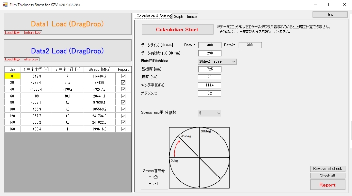
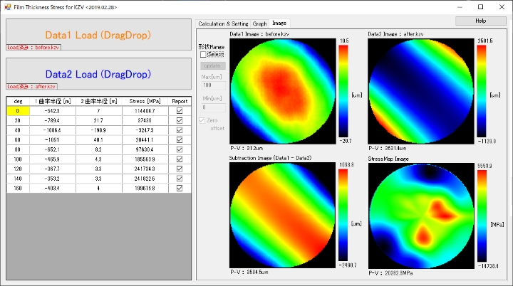
Post-deposition stress measurement application (optional)Measurement software for film stress distribution
Using SORI measurement data before and after deposition, the software specifies analysis lines in the wafer diameter direction and calculates the film stress distribution according to the radius of curvature and set parameters for each data. It also calculates profile data for each cross-section and outputs a report.