Wafer Profilometry Solutions
-
DY-2000RC/DY-3000RC
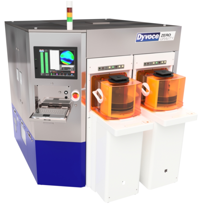
C to C is a cassette-to-cassette system for measuring the surface profile and thickness of semiconductor wafers. It realizes high-throughput measurement in the semiconductor process, and is customizable to measure the rim shape of TAIKO wafers and change the number of ports, etc. Cassette transfer using OHT with GEM support is also available.
Features- ・Cassette to Cassette (CtoC) support, high throughput
- ・Supports up to 12-inch wafers, SEMI standard measurement
- ・Compatible with SECS / GEM / GEM300
Various sensors for displacement/thickness measurement can be mounted.Numerous measurement sensors for geometry/thickness can be mounted- Sample Material
- Sample Type
- Measurement Item
-
DY-3001YM
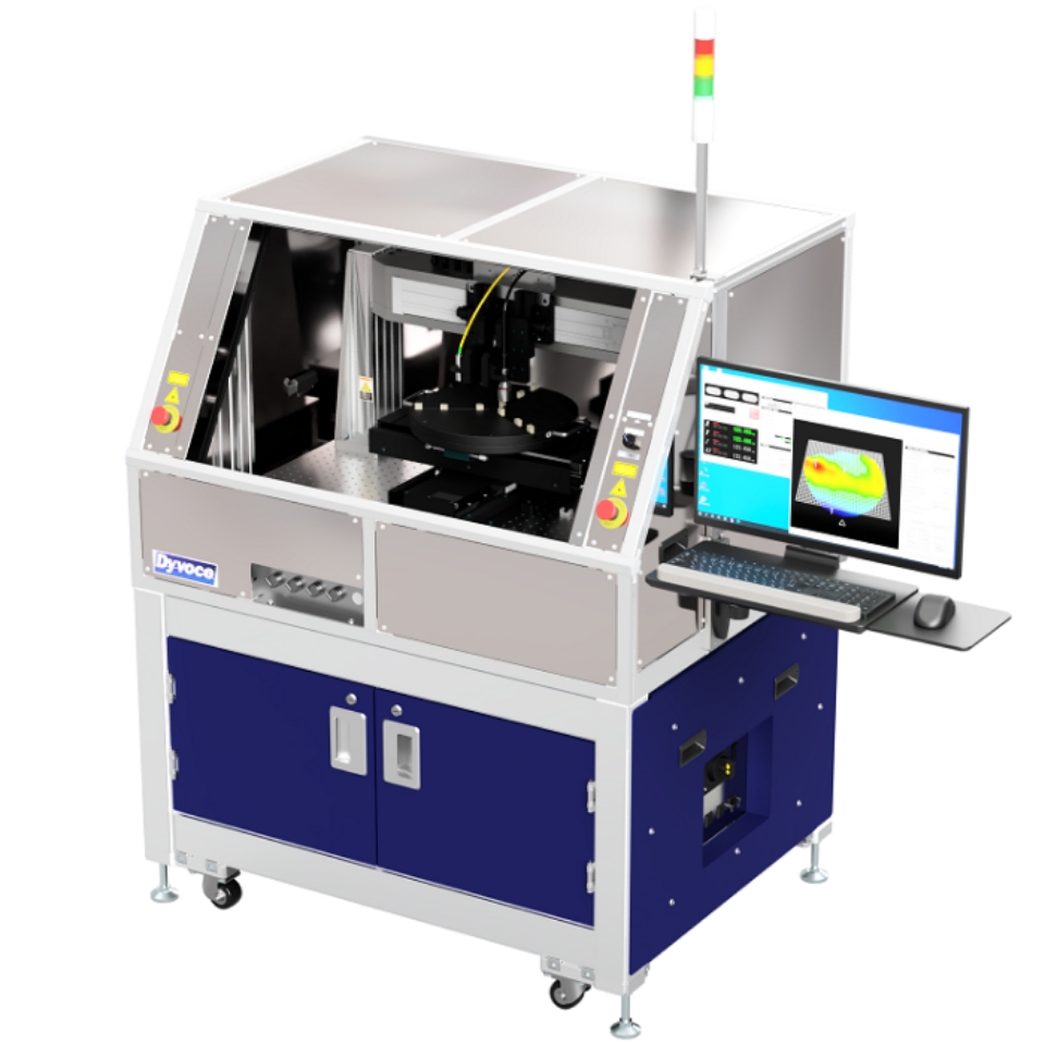
TThe manual single wafer type is a non-contact surface profile and thickness measurement system for not only hand-held semiconductor wafers but also various other samples. It is a basic unit that enables a variety of measurements with its high reliability and motion control technology, which only a high-precision stage manufacturer can provide, and is equipped with functions designed for ease of use and a simple user interface.
Features- ・Single-wafer type, applicable to various samples up to □300 mm, SEMI standard measurement
Various sensors for displacement/thickness measurement can be mounted.Numerous measurement sensors for shape/thickness can be mounted- Sample Material
- Sample Type
- Measurement Items
Rough crystallinity can be estimated from ingot curvature information.
Dyvoce can also measure the shape of ingots such as SiC.
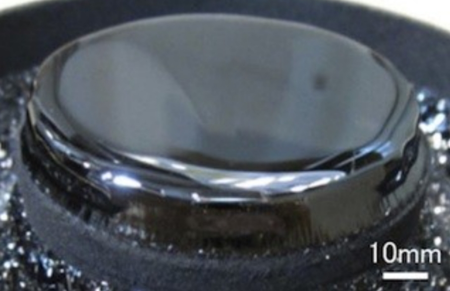
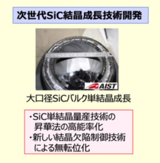
https://www.aist.go.jp/aist_j/news/pr20210309.html
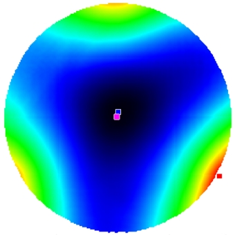
By looking at the warpage of wafers, it is possible to improve yield and diagnose the processing process in each process. Wafer warpage is either created during slicing or from the stress difference between the front and back sides of the wafer in subsequent processes. This is due to unevenness in the machining transformation layer created during polishing processes, for example, or film stress on the deposition surface during deposition processes; Dyvoce measurement data can be used to analyze this stress.
Depending on wafer warpage, there may be cases where the inline process cannot be used. For example, a suction error in the robot hand or the suction plate of the equipment. Dyvoce can mount the work table of a single-wafer machine to imitate the robot hand or the suction plate of each process device, so it is possible to evaluate an inline machine with an offline machine.
As the name implies, a wafer is a thin object, so the shape and amount of warpage of a wafer will vary depending on how the wafer is set against the equipment. This is especially true for wafers with low rigidity, such as large-diameter wafers and thin wafers. This is the reason why it is currently difficult to correlate warp shape and warp amount between different equipment. Therefore, Dyvoce can measure the warpage shape and amount of warpage of a wafer close to the true value by placing the wafer horizontally on three support points in the equipment and correcting for self-weight deflection based on the results of two measurements, one with the surface facing up and the other with the back side facing up. Also, by using model data, self-weight deflection can be corrected even if only one side of the surface is measured.
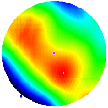
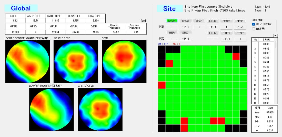
Using SORI profile measurement data before and after deposition, the software specifies analysis lines in the wafer diameter direction and calculates the film stress distribution according to the radius of curvature and set parameters for each data. It also calculates profile data for each cross-section and outputs a report.
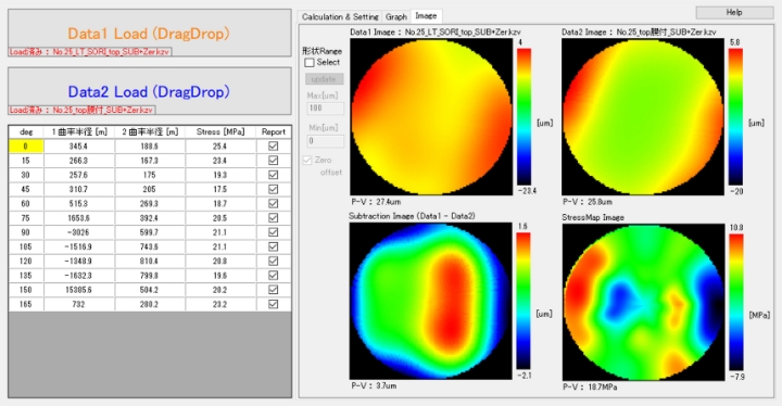
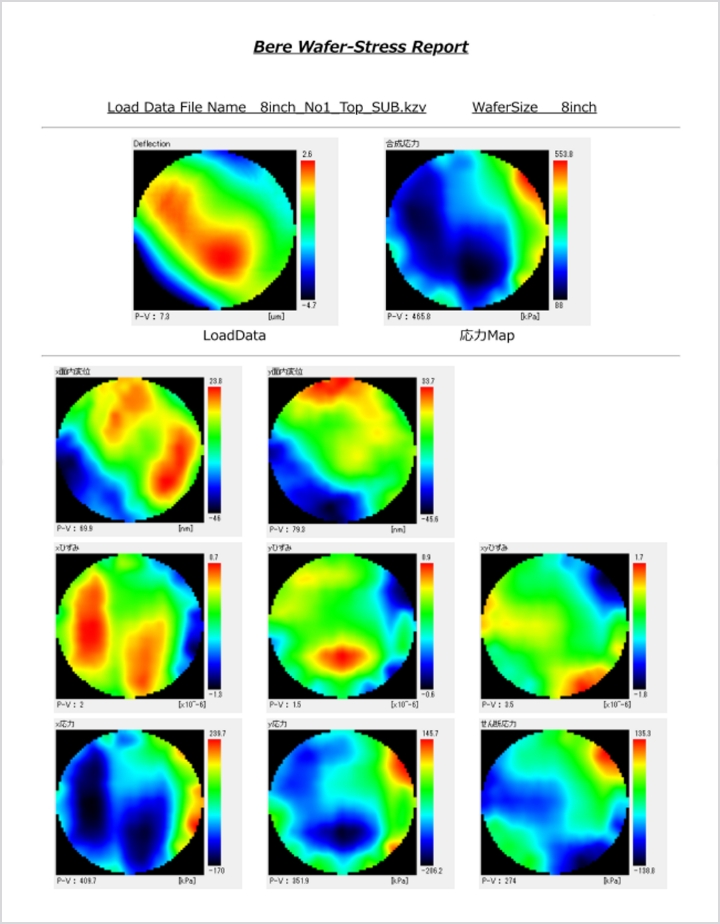
Analyzes the stress in a bare wafer based on the shape data of the wafer.
By looking at the thickness of a wafer, it is possible to improve yield in each process and diagnose the processing process. Lack of control of this thickness can lead to focus errors in the exposure process where the wafer is suctioned, etc.
The GBIR of each deposited film can be measured.
Cautions for Wafer Thickness MeasurementThere are various methods of wafer thickness measurement. Each has its own advantages and disadvantages, so care should be taken.
Unevenness of thickness at each site when cutting a wafer can be measured.